- 您现在的位置:买卖IC网 > Sheet目录324 > EK-V6-ML631-G-J (Xilinx Inc)VIRTEX-6 HXT FPGA ML631 EVAL KIT
�� �
�
�Virtex-6� FPGA� Data� Sheet:� DC� and� Switching� Characteristics�
�Table� 16:� GTX� Transceiver� Quiescent� Supply� Current� (per� Lane)� (1)(2)(3)�
�Symbol�
�I� MGTAVTTQ�
�I� MGTAVCCQ�
�Description�
�Quiescent� MGTAVTT� supply� current� for� one� GTX� transceiver�
�Quiescent� MGTAVCC� supply� current� for� one� GTX� transceiver�
�Typ� (4)�
�0.9�
�3.5�
�Max�
�Note� 2�
�Units�
�mA�
�mA�
�Notes:�
�1.�
�2.�
�3.�
�4.�
�Device� powered� and� unconfigured.�
�Currents� for� conditions� other� than� values� specified� in� this� table� can� be� obtained� by� using� the� XPE� or� XPA� tools.�
�GTX� transceiver� quiescent� supply� current� for� an� entire� device� can� be� calculated� by� multiplying� the� values� in� this� table� by� the� number� of�
�available� GTX� transceivers.�
�Typical� values� are� specified� at� nominal� voltage,� 25°C.�
�GTX� Transceiver� DC� Input� and� Output� Levels�
�Table� 17� summarizes� the� DC� output� specifications� of� the� GTX� transceivers� in� Virtex-6� FPGAs.� Consult� UG366� :� Virtex-6�
�FPGA� GTX� Transceivers� User� Guide� for� further� details.�
�Table� 17:� GTX� Transceiver� DC� Specifications�
�Symbol�
�DV� PPIN�
�V� IN�
�V� CMIN�
�DC� Parameter�
�Differential� peak-to-peak� input�
�voltage�
�Absolute� input� voltage�
�Common� mode� input� voltage�
�Conditions�
�External� AC� coupled� ≤� 4.25� Gb/s�
�External� AC� coupled� >� 4.25� Gb/s�
�DC� coupled�
�MGTAVTT� =� 1.2V�
�DC� coupled�
�MGTAVTT� =� 1.2V�
�Min�
�125�
�175�
�–400�
�–�
�Typ�
�–�
�–�
�–�
�2/3� MGTAVTT�
�Max�
�2000�
�2000�
�MGTAVTT�
�–�
�Units�
�mV�
�mV�
�mV�
�mV�
�DV� PPOUT�
�Differential� peak-to-peak� output� Transmitter� output� swing� is� set� to�
�voltage� (1)� maximum� setting�
�–�
�–�
�1000�
�mV�
�V� CMOUTDC�
�DC� common� mode� output�
�voltage.�
�Equation� based�
�MGTAVTT� –� DV� PPOUT� /4�
�mV�
�R� IN�
�R� OUT�
�T� OSKEW�
�Differential� input� resistance�
�Differential� output� resistance�
�Transmitter� output� pair� (TXP� and� TXN)� intra-pair� skew�
�80�
�80�
�–�
�100�
�100�
�2�
�130�
�120�
�8�
�Ω�
�Ω�
�ps�
�C� EXT�
�Recommended� external� AC� coupling�
�capacitor� (2)�
�–�
�100�
�–�
�nF�
�Notes:�
�1.�
�2.�
�The� output� swing� and� preemphasis� levels� are� programmable� using� the� attributes� discussed� in� UG366� :� Virtex-6� FPGA� GTX� Transceivers� User�
�Guide� and� can� result� in� values� lower� than� reported� in� this� table.�
�Other� values� can� be� used� as� appropriate� to� conform� to� specific� protocols� and� standards.�
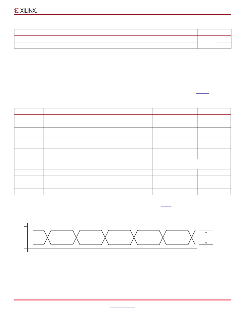
�X-Ref� Target� -� Figure� 1�
�+V�
�P�
�S� ingle-Ended�
�N�
�0�
�DS152� (v3.6)� March� 18,� 2014�
�Product� Specification�
�Figure� 1:� Single-Ended� Peak-to-Peak� Voltage�
��Volt� a� ge�
�d� s� 152_01_121509�
�12�
�发布紧急采购,3分钟左右您将得到回复。
相关PDF资料
EK-V7-VC707-CES-G
VIRTEX-7 VC707 EVAL KIT
EK-Z7-ZC702-CES-G
ZYNQ-7000 EPP ZC702 EVAL KIT
EL1848IYZ-T7
IC LED DRIVR WHITE BCKLGT 8-MSOP
EL7156CSZ
IC DRIVER PIN 40MHZ 3STATE 8SOIC
EL7158ISZ
IC DVR PIN 40MHZ 3STATE 8-SOIC
EL7222CSZ
IC DVR HS DUAL MOSFET 8-SOIC
EL7242CSZ
IC DVR HS DUAL MOSFET 8-SOIC
EL7243CMZ-T13
IC CCD DRIVER DUAL HS 20-SOIC
相关代理商/技术参数
EK-V7-VC707-CES-G
功能描述:VIRTEX-7 VC707 EVAL KIT RoHS:是 类别:编程器,开发系统 >> 通用嵌入式开发板和套件(MCU、DSP、FPGA、CPLD等) 系列:Virtex®-7 标准包装:1 系列:PICDEM™ 类型:MCU 适用于相关产品:PIC10F206,PIC16F690,PIC16F819 所含物品:板,线缆,元件,CD,PICkit 编程器 产品目录页面:659 (CN2011-ZH PDF)
EK-V7-VC707-CES-G-J
功能描述:VIRTEX-7 VC707 EVAL KIT JAPAN RoHS:是 类别:编程器,开发系统 >> 通用嵌入式开发板和套件(MCU、DSP、FPGA、CPLD等) 系列:Virtex®-7 标准包装:1 系列:PICDEM™ 类型:MCU 适用于相关产品:PIC10F206,PIC16F690,PIC16F819 所含物品:板,线缆,元件,CD,PICkit 编程器 产品目录页面:659 (CN2011-ZH PDF)
EK-V7-VC707-G
制造商:Xilinx 功能描述:VIRTEX-7 FPGA VC707 EVALUATION KIT - Boxed Product (Development Kits) 制造商:Xilinx 功能描述:KIT EVAL VIRTEX7 VC707 制造商:Xilinx 功能描述:VIRTEX-7 VC707 FPGA EVAL KIT
EK-V7-VC707-G-J
制造商:Xilinx 功能描述:KIT EVAL VIRTEX7 VC707 JAPAN
EKWF111
功能描述:WiFi/802.11开发工具 WF111 SDIO Eval kit
RoHS:否 制造商:Roving Networks 产品:Evaluation Boards 工具用于评估:RN-171 支持协议:802.11 b/g 频率:2.4 GHz 接口类型:UART 工作电源电压:2 V to 16 V
EKWT11-A
功能描述:蓝牙/802.15.1 开发工具 EKWT11-A
RoHS:否 制造商:Panasonic Electronic Components 产品:Bluetooth Evaluation Kit 工具用于评估:PAN1721 频率:2.4 GHz 接口类型:I2C 工作电源电压:2 V to 3.6 V
EKWT11-E
功能描述:蓝牙/802.15.1 开发工具 EKWT11-E
RoHS:否 制造商:Panasonic Electronic Components 产品:Bluetooth Evaluation Kit 工具用于评估:PAN1721 频率:2.4 GHz 接口类型:I2C 工作电源电压:2 V to 3.6 V
EKWT11i-A
功能描述:蓝牙/802.15.1 开发工具 WT11i A Eval Kit
RoHS:否 制造商:Panasonic Electronic Components 产品:Bluetooth Evaluation Kit 工具用于评估:PAN1721 频率:2.4 GHz 接口类型:I2C 工作电源电压:2 V to 3.6 V